
SPECIAL SESSIONS
“OpenPDK - Global FOSS Scholar Platform"
The OpenPDK initiative delivers a global FOSS Scholar Platform supporting analog/RF, mixed‑signal, and digital IC design. Central to this effort are accurate SPICE models for low‑power sensing MOSFETs, RF HBTs, and emerging RRAM devices, validated across cryogenic temperatures for space and quantum‑computing applications. The initiative also advances Verilog‑A compact‑model standardization, ensuring result reproducibility and seamless integration into open‑source design flows. Supported by the EU Chips JU, OpenPDK fosters collaboration among academia, startups, and industry, while providing FOSS IC‑design tools covering schematic capture, simulation, layout, and verification up to tape‑out. Similar to the EU Chips JU program, Zhejiang CoreXin in China offers an open‑source PDK together with tape‑out services for its 55 nm process. To accelerate the semiconductor‑industry development across the Asia‑Pacific and Southeast‑Asia regions, semiconductor model development and parameter extraction techniques should be pursued in a more focused manner. This special session brings together experts to present and discuss advances in device characterization, compact modeling, simulation methodologies, and validation techniques for a broad range of solid‑state devices, including Si, III/V semiconductors, power devices, nanoscale structures, and emerging 2.5D/3D advanced packaging technologies.
Presenters
- MOS-AK and Verilog-A standard model and practice, Dr. Wladek Grabinski,GMC Consulting, Switzerland
- Open-Source Ecosystem Updates and Semiconductor Design Development Programs in Japan, Mr. Jun-ichi Okamura, AIST Solutions, OpenSUSI, Japan
- Open-Source EDA Meets Industrial IC Design, Ehrenfried Seebacher, ams-OSRAM AG, Austria.
- Building an Open-Source Process Platform,Empowering VLSI Innovation and Development, Prof. Da Zhang, Zhejiang University/CTO, Zhejiang Chuangxin Integrated Process Platform, China
- From Silicon to Design: Intelligent Measurement and Modeling for DTCO, Dr. Yutao Ma, VP of R&D, Primarius Technologies. Ltd. China
- Beyond Moore, Application-Driven IC Innovation International Cooperation Opportunities at NICE, Prof. Alex Gu, National Innovation Center Par Excellence (NICE), China
- 2.5D/3D IC: AI+EDA Reshaping the System–Design–Technology Co-Optimization (STCO) Paradigm for Advanced Packaging, Dr. Alex Zhao, Founder/CEO Zhuhai SiChip Technology Co., Ltd., China
- Modelling of semiconductor devices: the heart of innovation bridging academia and industrial applications, Prof. Fujiang Lin, University of Science and Technology of China (USTC), China
Panel discussion: How to have a close loop for PDK, EDA, PDA and ICS simulation?
“OpenPDK - Global FOSS Scholar Platform"
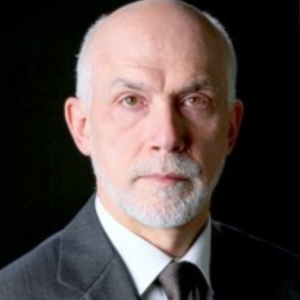
GRABINSKI Wladek
GMC Consulting, , 瑞士
传
Wladek Grabinski received the Ph.D. degree from the Institute of Electron Technology, Warsaw, Poland, in 1991. From 1991 to 1998 he was a Research Assistant at the Integrated Systems Lab, ETHZ, Switzerland, supporting the CMOS and BiCMOS technology developments by electrical characterization of the processes and devices. From 1999 to 2000, he was with LEG, EPFL, and was engaged in the compact MOSFET model developments supporting numerical device simulation and parameter extraction. Later, he was a technical staff engineer at Motorola, and subsequently at Freescale Semiconductor, Geneva Modeling Center, Switzerland. He is now a consultant responsible for SPICE modeling, characterization and parameter extraction of MOST devices for the analog/RF IC applications. He is currently consulting on the development of next- generation compact models for the nanoscaled technology very large scale integration (VLSI) circuit simulation. His current research interests are in high-frequency characterization, compact modeling and its Verilog-A standardization as well as device numerical simulations of MOSFETs for analog/RF low power IC applications. He is an editor of the reference modeling book Transistor Level Modeling for Analog/RF IC Design and also authored or coauthored more than 50 papers. Wladek is the chair of the ESSDERC Track4: “Device and Circuit Compact Modeling” as well as has served as a member of organization committee of ESSDERC/ESSDERC, TPC of SBMicro, SISPAD, MIXDES Conferences; reviewer of the IEEE TED, IEEE MWCL, IJNM, MEE, MEJ. He is a Member At Large of Swiss IEEE ExCom and also supports the EPFL IEEE Student Branch acting as its Interim Branch Mentor. Wladek is involved in activities of the MOS-AK Association and serves as a coordinating manager since 1999.
Abstract
The semiconductor industry has been evolving and innovating for nearly a century, ever since the invention of the first transistor. This rapid growth is driven by the direct and proactive contribution of OpenSilicon CAD/EDA to the entire technology flow: from state-of-the-art semiconductor technologies and device-level compact/SPICE modeling to Verilog-A standardization and advanced IC designs for various high-tech applications. However, the semiconductor industry also faces significant challenges in sustaining a workforce of skilled technicians and engineers. To address the increasing global demand for well-trained talent, innovative pathways must be established to attract professionals and strengthen local microelectronics ecosystems. The OpenSilicon CAD/EDA platform, established using recently released OpenPDKs, provides a powerful new scholar framework to connect beginners, enthusiasts, and experienced mentors, allowing them to benefit from the fast-growing open-source IC design movement. Indeed, collaborative OpenSilicon IC design is increasingly viable due to the rapid growth of OpenPDKs offered by SkyWater, GF, ICsprout55, ToakiRikita, SCL and IHP. This talk highlights how the European Chips JU ODE4EC-AMS Project coordinates and strengthens Europe’s OpenSilicon CAD/EDA ecosystem to advance SPICE/Verilog-A modeling and standardization, integrating a complete open-source IC design flow (Xschem, Qucs-S, ngspice, Xyce, OpenVAF, OpenEMS, Magic, KLayout, LibreLine), and showcasing representative analog/RF and digital IC design examples manufactured through this collaborative effort.
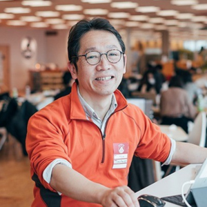
Jun-ichi OKAMURA
AIST Solutions, OpenSUSI, 日本
传
Jun-ichi OKAMURA began his career at Toshiba in 1986 as a DRAM memory designer and later worked at IBM in Burlington, Vermont, on alliance programs related to the first-generation DDR SDRAM.
In 1999, he joined THine Electronics as a lead SerDes designer in the fabless semiconductor business. In 2006, he founded Trigence Semiconductor, which received its first investment from Intel Capital in 2012. Unfortunately, due to the impact of the U.S.–China trade war, Trigence was unable to secure Series D funding and was legally liquidated in May 2022.
After being invited to the National Institute of Advanced Industrial Science and Technology (AIST) as a guest researcher, he joined AIST Solutions in June 2023, where he has been engaged in semiconductor ecosystem development and policy planning activities.
In April 2024, he became the Representative Director of OpenSUSI (Open Source Utilized Silicon Initiatives), where he promotes semiconductor design talent development and the growth of the open-source silicon ecosystem in Japan.
Abstract
Since October 2025, we have been publicly releasing the Tokai Rika 1 µm CMOS technology as an open-source PDK via the OpenSUSI repository. In this talk, I will first present the latest status of the open-source PDK development, including the key technical issues that have emerged and our ongoing efforts to refine and improve the overall methodology. I will then introduce the “First Tapeout” proposal in 2026 as a talent identification and development program. This initiative represents Japan’s first attempt to provide hands-on experience covering the full RTL-to-GDSII-to-chip flow in collaboration with industrial partners. Finally, I will outline the OpenSUSI MPW shuttle program released for 2026, which aims to engage Japanese academia and further strengthen practical semiconductor design and fabrication experience.

Ehrenfried SEEBACHER
ams-OSRAM AG, Austria
传
Ehrenfried Seebacher is Senior Director of Research & Development at AMS-OSRAM, where he leads innovation activities in semiconductor technologies, design methodologies, and advanced product development. He has extensive experience in analog, mixed-signal, high-voltage, sensor, and automotive integrated circuits, spanning both semiconductor manufacturing and IC design environments. He is a Senior Member of the IEEE and has been actively involved in numerous European and international collaborative research projects, fostering cooperation between industry, universities, and research institutes. His work focuses on bridging academic innovation with industrial semiconductor development, including emerging topics such as compact modeling and process characterization, open-source EDA, open PDK enablement, design automation, and next-generation IC design methodologies.
Through his engagement with universities, EU-funded research initiatives, and international technology networks, he actively promotes knowledge exchange between academia and industry to accelerate innovation and strengthen Europe’s semiconductor ecosystem.
Abstract
Open-source EDA tools and PDKs have become an important driver for semiconductor innovation, education, and collaborative research. While universities successfully utilize open-source ecosystems for teaching and prototyping, industrial semiconductor development requires significantly higher standards regarding analog/MS simulation, verification, qualification, reliability, IP protection, and sign-off quality.
This presentation provides an industrial perspective from ams-OSRAM on the adoption of open-source EDA technologies in professional IC development environments. We discuss the opportunities and limitations of current open-source analog and digital design flows, the challenges of integrating industrial PDKs, and the role of open-source tools as complementary solutions alongside established commercial EDA platforms.
The talk highlights practical experiences, industry-academia collaboration models, and a roadmap for leveraging open-source technologies to accelerate innovation, improve accessibility, and strengthen the resilience of semiconductor design ecosystems while maintaining industrial quality requirements.
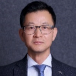
Dr. Da ZHANG
Zhejiang University/CTO, Zhejiang Chuangxin Integrated Process Platform, 中国
传
Dr. Da Zhang is a Qiushi Distinguished Professor at the School of Integrated Circuits, Zhejiang University. He has long been engaged in R&D and productizations in the integrated circuit industry. Prior to joining Zhejiang University this year, Dr. Zhang served as an Executive Director at Synopsys in the United States, where his responsibilities include advanced node process co-development, sensor IP design, and silicon lifecycle management development. Before that, he accumulated years of valuable management and R&D experience at leading companies including AMD and Freescale, witnessing and contributing to key evolutions in the semiconductor industry. Dr. Zhang received his bachelor’s and master’s degrees from Zhejiang University and his Ph.D. from the University of Illinois at Urbana-Champaign. He holds 32 U.S. patents.
Abstract
Due to the high complexity and strong interdependence of integrated circuit (IC) design and manufacturing, new architectures and design concepts require comprehensive, systematic tape-out verification and iterative tuning in order to progressively reach product level maturity. However, the industry has long been constrained by closed PDK (Process Design Kit) ecosystems and high tape out costs, which have significantly hindered broad based innovation in the IC field.
This presentation introduces the pioneering work undertaken by Zhejiang University and the Chuangxin Integrated Circuit Process Platform in building an open source PDK/tape out ecosystem, as well as effective practices for empowering industrial innovation and development. Based on the newly established full scale 12 inch production line, the platform has developed high quality CMOS processes and is extending into various impactful specialty process domains. The process technologies developed by the platform are open to the public to empower the industry. In collaboration with the Institute of Computing Technology, Chinese Academy of Sciences, the platform has formed a full chain open source ecosystem encompassing design, IP, and PDK. This open source ecosystem strongly supports high quality talent development, novel concept validation, and large scale industrial enablement.
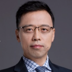
Dr. Yutao MA
VP of R&D, Primarius Technologies. Ltd., 中国
传
Dr. Yutao Ma received his bachelor’s degree in 1996 and his Ph.D. in 2001, both in Microelectronics from Tsinghua University. He has since worked in the EDA industry for over 20 years, from Celestry to Cadence and then Primarius. His expertise includes semiconductor device modeling, circuit simulation, and yield analysis. Dr. Ma is currently Vice President of R&D at Primarius Technologies, where he leads technology innovation, new product development, and the R&D engineering infrastructure team. He also serves as Director of the EDA Innovation Key Laboratory of Shandong Province and Co-Director of the Primarius-Peking University DTCO Innovation Laboratory. Dr. Ma has published dozens of technical papers in leading journals and conferences and holds multiple patents in device modeling, simulation algorithms, yield analysis, and hardware acceleration.
Abstract
Advanced semiconductor technologies are transforming device characterization and modeling from model-delivery tasks into critical infrastructure for DTCO. This talk presents a “silicon-to-design” loop spanning multi-domain measurement, compact modeling, parameter extraction, model QA, and circuit simulation. Challenges in FinFET/GAA, RF, reliability, and dynamic-bias noise are discussed, together with how automation and AI can improve modeling efficiency under physics-based constraints and rigorous governance. Primarius’ integrated capabilities in measurement, modeling, automated extraction, QA, and simulation are used to illustrate a practical path toward intelligent, learning-based model development for DTCO.
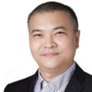
Prof. Alex GU
National Innovation Center Par Excellence (NICE), 中国
传
Prof. Alex Gu is a Vice President of the National Innovation Center Par Excellence (NICE), overseeing the MicroNano and Integrated Circuit Division, as well as the Overseas and Hong Kong/Macao/Taiwan Cooperation Department. Prior to his current post, Prof. Gu was the founding Dean of the School of Microelectronics at Shanghai University, the Deputy Executive Director of the Institute of Microelectronics (IME) Singapore, and a Principal Scientist at Honeywell International, Inc. (Minnesota, USA). Prof. Gu brings 20+ years of experience in R&D, Education, Management and Commercialization. Prof. Gu’s research interest is in the field of Micro Electro Mechanical Systems (MEMS), primarily in Aluminum Nitride (AlN) – based functional thin films and related MEMS sensors. Prof. Gu is a class 1998 PhD alumni of the University of Minnesota.
Abstract
This report presents the strategic landscape and international cooperation opportunities for application-driven integrated circuit (IC) innovation in China’s Yangtze River Delta, facilitated by the National Innovation Center par Excellence (NICE). Despite possessing the nation’s most complete IC industrial chain, the region faces challenges including advanced process gaps, reliance on imported equipment, and insufficient industrial synergy. To address these, NICE operates a “Grant-to-Equity” model to de-risk early-stage ventures and focuses its R&D portfolio on a “Beyond Moore” strategy—encompassing wide-bandgap power devices, advanced packaging/Chiplet, silicon photonics, and MEMS—to build a distinctive specialty process and pilot-test supply chain driven by real-world applications in automotive, AI, and industrial sectors. Through case studies and a commitment to open global partnerships, NICE aims to bridge the gap between research and commercialization, overcome high-end technology bottlenecks, and co-build a resilient and collaborative innovation ecosystem with international partners.
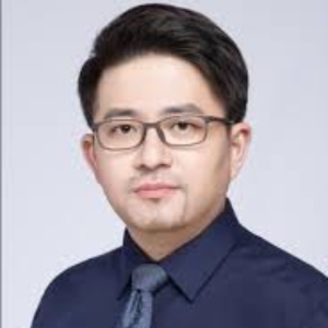
Dr. Alex ZHAO
Founder/CEO Zhuhai SiChip Technology Co., Ltd., 中国
传
Dr. Zhao holds a PhD from the University of Southampton, UK, where he studied under Prof. Bashir Al-Hashimi, Fellow of the Royal Academy of Engineering. He began research on 2.5D/3D stacked-chip design in 2008 as a member of one of the world’s earliest teams chip-architecture design methodologies.The team subsequently completed 3D-IC validation in collaboration with IMEC. With 15 years of dedicated experience in design and development, Dr. Zhao has published numerous papers at leading international venues and received the VLSI-SoC International Best Paper Award. He currently serves as Founder and Chief Scientist of Zhuhai SiChip Technology Co., Ltd., where he leads projects under China’s National Key R&D Program and directs his team in the independent research and development of 2.5D/3D stacked-chipEDAsoftware, driving breakthroughs in the semiconductor industry through full-flow back-end EDA tools and solutions.
Abstract
By reconfiguring chip stacking and interconnect, 2.5D/3D IC technology overcomes the bottlenecks of conventional planar integration, but it also introduces unprecedented system complexity—spanning micro-bump pitch, through-silicon via (TSV) density, and—which steadily widens the gap between design and manufacturing process.
This presentation focuses on a new paradigm of System-Technology Co-Optimization (STCO) driven by the dual engines of “AI + EDA.” First, we will analyze the coupling mechanisms between design rules and process windows in 2.5D/3D ICs,exposing the efficiency bottleneck inherent in the traditional serial design-process iteration model. , we will explore how large-scale AI models can empower the EDA toolchain to enable full-flow intelligence—from architecture exploration and place-and-route to package signoff, thereby achieving rapid convergence to optimal solutions within ultra-large search spaces. Finally, we will share practicalSTCO implementations in representative scenarios such as High Bandwidth Memory (HBM) and chiplet-based designs, demonstrating how early process-aware design optimization and manufacturability-driven architectural innovation can deliver systematic breakthroughs in PPPAC . We look forward to exploring the new frontiers of advanced packaging together with.

Prof Fujiang LIN
University of Science and Technology of China (USTC), 中国
传
Fujiang Lin,Professor at the University of Science and Technology of China (USTC); Former Vice Dean of the School of Microelectronics; Senior Consultant at the Jiangsu Industrial Technology Research Institute Innovation Centre.
Prof. Lin earned his bachelor’s and master’s degrees as a member of USTC’s Class of 1977, followed by his doctoral degree in West Germany. Under Singapore’s EDB Scheme, he relocated to Singapore in 1993. He has worked at numerous cross-border industrial, academic and research institutions and successfully founded the startup Transilica. In 2009, he was selected as a National Distinguished Innovative Talent and returned full-time to his alma mater USTC. He served as Executive Director of the 23rd Department and co-founded China’s National Demonstrative School of Microelectronics. He has supervised nearly 200 graduate students, published more than 200 academic papers, and holds over 80 invention patents.
His primary research interests cover microwave technology, micro-nano device modeling, wireless communication chip design, and optoelectronic chip design, with more than 30 years of extensive international experience in industry-academia-research collaboration.
In the industrial sector, he previously served as an independent director of Shanghai Fudan Microelectronics Co., Ltd., and was the founder and Chairman of Jiangsu Kedahengxin Semiconductor Pte., Ltd., leading his team to develop electrical chips for optical communication.
Prof. Lin is a co-founder of two international IEEE conferences: IEEE RFIT and IEEE ICTA.
Abstract
Thirty-seven years ago, the speaker’s doctoral dissertation in West Germany addressed the consistency issue of parameter extraction for microwave device modeling—a challenge that remains prevalent to this day. Upon completing his PhD, the speaker relocated to Singapore. He subsequently carried out pioneering research on modeling, parameter extraction and chip design for state-of-the-art semiconductor devices at several renowned cross-border institutions, including Singapore’s Institute of Microelectronics (IME), the HP EEsof Semiconductor Modeling Center in Singapore, and the SPICE team of Chartered Semiconductor Manufacturing. His technical contributions enabled a one-pass success of an RF chip development project. Drawing on nearly four decades of experience in semiconductor device modeling, this talk will share practical modeling methodologies, persistent technical bottlenecks, and validated strategies for effective parameter extraction accumulated throughout his career. Also will share his effort to bring modeling activity in R10/R11 to align with the international compact model coalition.